The CRPG Scanning Electron Microscope and Microprobe facility (Microscopie et microsonde électronique, MeMi) performs qualitative, semi-quantitative and quantitative imaging of terrestrial, extraterrestrial and experimental geological materials using a scanning electron microscope and electron microprobe.
At the local level, this facility is part of the ANATELo (OSU OTELo) and ICÉEL (Institut Carnot) networks and is supported by LabEx Ressources21.
Book a session (CRPG users)
Standards available
Equipment
Electron microprobe (EPMA)
JEOL JXA 8230
Description:
In 2021, the CRPG acquired a JEOL JXA 8230 electron microprobe. This machine is dedicated to quantitative chemical mapping. The electron gun uses a tungsten filament, and the accelerating voltage can be varied between 0.2 and 30 kV, depending on the required use.
This microprobe is equipped with 5 wavelength dispersive spectrometers (WDS), each with 2–4 crystal monochromators and a P-10 or Xenon X-ray counter. This configuration allows precise, in-situ quantitative analyses of all elements from Boron to Uranium. Furthermore, an energy dispersive spectrometer (EDS) allows the rapid identification of elements and can be used in conjunction with the other spectrometers for simultaneous analyses of elements present at very different concentrations.
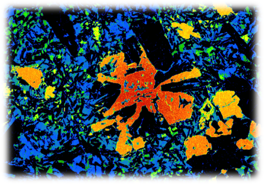
Secondary electron (SE) and backscattered electron (BSE) detectors are used to acquire images at magnifications from 40× to ~100,000×.
BSE images reveal compositional contrasts based on the molecular mass (average Z) of the sample at the scanning level. A panchromatic cathodoluminescence (CL) detector is also attached to the microprobe, which efficiently reveals zoning defects in crystals (for example in olivine, quartz, zircon, apatite…).
The volume of interaction between the beam and the sample depends on the analytical conditions, but is estimated to be 1 µm3 for classical analyses of silicates; this volume is reduced at lower accelerating voltages and higher sample densities. That said, if very mobile (e.g. alkaline) elements are being analysed, the beam can be defocused to 20 µm in diameter.
Detection limits also depend on the analytical conditions (they are higher for lighter elements, i.e. from Boron to Fluorine) and are generally between 10 and 200 ppm.
The wide range of analysable elements is made possible by the CRPG’s extensive catalogue of very well characterised standards.
Analytical samples must be solid and preferentially in perfectly polished thick or thin sections (ideally 1” in diameter). For non-conductive samples (natural rocks, experimental silicate samples…), a carbon coat 20–30 nm thick is necessary to evacuate incident electrons.
Analyses:
Point-by-point quantitative analyses: all elements present are quantified to determine the composition of the sample at the analytical point (~1–20 µm in diameter).
Qualitative and quantitative elemental mapping: the spatial (2D) distribution of selected elements is obtained by scanning the surface and is represented in single- or multi-elemental maps. Chemical maps spanning multiple centimetres can be obtained in our facility.
Scanning electron microscope (SEM)
JEOL 6510
Description:
Since 2010, the CRPG has housed a JEOL 6510 SEM with a tungsten filament. This instrument is principally used for imaging and is equipped with SE and BSE detectors that are used to acquire high-quality electron images at magnifications up to 50,000× (depending on the analytical conditions).
This instrument is also equipped with a Gatan CL detector to observe mineral structures. A Bruker CrystAlign400 electron backscatter diffraction (EBSD) system with an e-Flash detector is also installed on this instrument.
The wide range of possible accelerating voltages (0.2–30 kV) and the low probe current (typically a few pA), which is lower than that of the microprobe (tens to hundreds of nA), permits analyses of more fragile materials.
Rapid, semi-quantitative chemical analyses are also made possible by the coupled 30-mm2 Bruker XFlash 5030 energy-dispersive X-ray spectrometer.
Analytical samples must be solid (rocks, synthetic samples, metals…) and should be conductive or conductively coated to avoid the electric charges inherent to electron bombardment. Samples must also be vacuum-resistant (to ~10–5 mbar) because this SEM does not operate under partial vacuum.
It is possible to image un-polished samples, although the results are better on polished samples or thin sections.
Furthermore, the large chamber of the SEM can accommodate multi-centimetre samples (as long as the surface is electrically conductive), making this instrument very versatile.
Uses:
Rapid recognition of mineral phases in natural and synthetic samples.
Documenting mineral textures and structures.
Acquisition of electron and elemental distribution maps, with the possibility of programming multiple images and reconstructing a global map of the sample.
Characterisation of samples destined for other instrumental analyses (SIMS, LA-ICP-MS, microprobe…) and a posteriori verification of analytical points.
Access: Access to this facility is obtained by contacting the facility manager, who will evaluate the feasibility of the project (contact the manager by mail or using the request form below).
Pour offrir les meilleures expériences, nous utilisons des technologies telles que les cookies pour stocker et/ou accéder aux informations des appareils. Le fait de consentir à ces technologies nous permettra de traiter des données telles que le comportement de navigation ou les ID uniques sur ce site. Le fait de ne pas consentir ou de retirer son consentement peut avoir un effet négatif sur certaines caractéristiques et fonctions.
Fonctionnel
Always active
Le stockage ou l’accès technique est strictement nécessaire dans la finalité d’intérêt légitime de permettre l’utilisation d’un service spécifique explicitement demandé par l’abonné ou l’utilisateur, ou dans le seul but d’effectuer la transmission d’une communication sur un réseau de communications électroniques.
Préférences
Le stockage ou l’accès technique est nécessaire dans la finalité d’intérêt légitime de stocker des préférences qui ne sont pas demandées par l’abonné ou l’utilisateur.
Statistiques
Le stockage ou l’accès technique qui est utilisé exclusivement à des fins statistiques.Le stockage ou l’accès technique qui est utilisé exclusivement dans des finalités statistiques anonymes. En l’absence d’une assignation à comparaître, d’une conformité volontaire de la part de votre fournisseur d’accès à internet ou d’enregistrements supplémentaires provenant d’une tierce partie, les informations stockées ou extraites à cette seule fin ne peuvent généralement pas être utilisées pour vous identifier.
Marketing
Le stockage ou l’accès technique est nécessaire pour créer des profils d’utilisateurs afin d’envoyer des publicités, ou pour suivre l’utilisateur sur un site web ou sur plusieurs sites web ayant des finalités marketing similaires.